Development of a Simple Programmable Control Timer
Jonathan Gana KOLO and Umar Suleiman DAUDA
Department of Electrical and Computer Engineering, Federal University of Technology, Minna, Nigeria.
E-mail(s): jgkolo@gmail.com, usdauda@gmail.com
Abstract
Conserving electricity has become increasingly important as energy rates and shortages have increased. Consumers can find a number of ways to cut back on their electrical use, especially with appliances commonly found in the home.
Any economy that wants to advance must therefore embrace time management and proper conservation of electrical power supply. This can be achieved through limiting wastage in the limited power supply.
The programmable control timer can be use to put ON or OFF any electrical appliance connected to it while the user attends to other things knowing fully well that Electronic Assistance is available.
The user can preset the device to a certain value. This is possible with the use of set button on the device. The set button must be pressed to enable the time input buttons to be pressed. After presetting a certain time value, which is shown on the digital display, a press on the count button makes the preset time to countdown to zero. After attaining a “000” value, the appliance connected to its output sockets goes either ON or OFF.
Keywords
Timer, Latch, Oscillator, Switching Transistor, Counter.
Introduction
A control timer is intended to provide controls for processing, manufacturing, and domestic appliances based on exact timing, in areas where the measurement of time is critical to successful operation without intermittent human input [1]. It is quite evident that for proper organization, events should be done in specific time [2]. For ease, there are specific machines designed to alter or perform some defined task at particular instances. A good example is a “Timer”. It is tasked to trigger ON or OFF an event at a time. It is quite useful in everyday life. A simple example is in the case of clocks incorporating its application to alert people at a time by triggering on an alarm. Some advanced electronic timers are used for military purposes. Away from Military into Civilian life, timer has proved to be of great importance in microwave ovens, computer systems, laboratory experiments, heaters, etc. Besides, there are several industrial practices that would not go well without the presence of a timer [1].
This paper involves the design and construction of a programmable control timer, which is designed to count down a preset time to zero and trigger ON or OFF the output load. The programmable feature allows it to work with different time inputs and for this prototype the time does not exceed 999 seconds (16.65 minutes).
This design involves the use of a 4060B CMOS integrated circuit that takes the task running a 32768Hz crystal [3][4]. The input frequency (32768Hz) is divided by the internal dividers in the 4060B integrated circuit. The division results into 2Hz. An additional flip-flop is added to provide the needed 1Hz (or 1 second period pulse). This leading pulse passes through control logic before it is fed into a down counter unit. The Counter Unit consists of three BCD down counters that is assigned a particular preset number through the control logic. The Control Unit is made of latches or flip-flops. External switches are connected to the specific inputs of the flip-flops to provide specific controls. Furthermore, the counter unit is set to count down through the control unit. When a zero value is reached, a zero detector signals the state and feedbacks to the control unit, thereby resulting into the output load being triggered ON or OFF. The timer alters the electric power supply to the output load through an external relay circuit. This provides better switching performance and higher load capacity.
The other feature in the leading design is a crystal CMOS oscillator. A 555 timer cannot work for precision. Precision operation is very certain in crystal type oscillator. In the design, the oscillator works on 32768Hz crystal and through supported internal frequency dividers of the involved integrated circuit, a 1Hz frequency is achieved in clocking the counters. The timing technique reduces any effect of frequency instability.
The design is based on readily available electronic components that are in cheap supply. Therefore the overall cost of construction is indeed economical.
The programmable control timer’s uniqueness is found in its ability to switch ON and OFF an electrical load connected to it after a preset time.The system is divided into six functional units as shown in the block diagram of figure 1.
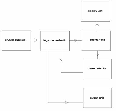
Figure 1. The block diagram of the programmable control timer
Crystal Oscillator
The crystal oscillator of Figure 2 (Configuration of the 4060B as a crystal oscillator) is a 4060B integrated circuit with few external electronics components. The device has reasonable frequency stability.
It has in-built 14-stage counter/divider logic that merely divides the main frequency down to lower values. Through this technique, the 4060B generates ten frequencies at once. All the outputs are buffered for heavy load driven ability. Its pin 12 should be grounded for the device to work. The frequency of the ten outputs is given by the following formula [5-9]:
|
|
x is the Q value of a particular output terminal.
In the case of this project, crystal frequency is 32768Hz. Therefore, the frequency output at pin 3 is given by:
|
|
Pin 3 is related to Q value of 14
For pin 1
|
|
These two terminals are used for circuit design.
This unit simply generates precision frequencies of 2Hz and 8Hz for this design.
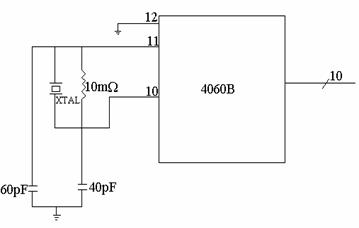
Figure 2. Configuration of the 4060B as a crystal oscillator
Logic Control Unit
Figure 3 is the logic diagram of the logic control unit which forms the central part of the system design. The unit is designed to further divide the frequency outputs from the crystal oscillator, control the counters and also to operate the output’s load. This unit embodies latch logic functions.
The logic control unit holds four latches. The 4013B 1 and 2 are divide by 2 configured latches. 4013B 1 divides the 2Hz pulse from the crystal oscillator to 1Hz. This resulting signal is aimed for counting purpose. Its period is evidently 1 second.
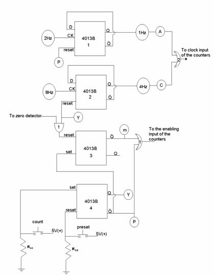
Figure 3. The Logic Control Unit
This timing provides 1 second timing for the counter unit. 4013B 2 divides the 8Hz signal from the crystal oscillator. The resulting 4Hz pulse is used for presetting the counter. Interestingly, the two latches are used for control purpose. Their reset terminals are useful for such control. The control involves raising a particular reset input to HIGH logical level. This results in disenabling the latch.
4013B 3 and 4 are used for device control. 4013B 3 deals with the output control. It responds, the instant the counter is at the lowest state i.e. “000”. 4013B 4 is the main latch. It controls every logic unit in the circuit. It has external inputs involving two soft touch buttons. Whenever any of the buttons is pressed, a HIGH logical level signal is sent to the corresponding input of the latch. One button is used for count CONTROL while the other for PRESET functions. The buttons works in accordance with basic SR latch or flip-flop’s truth table. One button must be pressed at a time.
When the preset button is pressed, 4013B 4 is reset. The result Q- brings out HIGH logic level, while Q is low. The terminal P output makes 4013B 1 disabled and 4013B 2 enabled. Therefore, OR gate 2 has 4Hz to clock the input of the counters. The 1Hz signal is cut-off. The OR gate 1 is high due to terminal P.
AND gate 1 is disabled during the preset action. This prevents the accidental triggering of the output by the zero detector. When the count button is pressed, 4013B 4 is set. Its Q output changes from logic 0 to 1 and Q- is low. In this case, the output of OR gate 1 is low. Now, 4013B 1 is enabled, while 4013B 2 is disabled. The output of the OR gate 2 is 1Hz. This is a 1 second period timing for counting down the counter unit.
AND gate 1 output is logical 1 when terminal Y is high and a high signal is sent from the zero detector. Y is high when 4013B 4 is at the count mode i.e. Q is high.
The PRESET mode is used for entering a particular digit or time into the counter unit at a relatively high speed (0.25 second period). The COUNT mode is a free-running operation of the counter. The Counter decrement every one-second.
Counter Unit
The Counter Unit of Figure 4 holds three 4029B BCD down counter. The counters are systematically and synchronously cascaded. The maximum count is 999 seconds or 16.65 minutes. The cascading of the counters is done in such a way that individual counter can be preset to a particular digit through buttons. Each counter has a preset button.
The configuration of the 4029B allows pin 7 (carry-out) to go low whenever a particular counter is at the lowest digit i.e. “0”. The output is low logical level for the integrated circuit to be functional.
A 2-input AND gate is used to preset each counter. Three of such gate is used in the circuit, one for each counter. These are AND gate 2, 3 and 4.The AND gates are connected as shown in Fig. 4. One of the input of the AND gate is connected to a particular pin 7 of a 4029B. The other input is connected to the positive (5V) through a 10KΩ resistor. The resistors put the inputs of the AND gates to high logical level. The result is normally carry-in to carry-out flow. The current status of the AND gate allows normal cascading of the counters.
When the 4013B 4 is at the preset mode, terminal Y is low. This allows the outer terminals of the switches to be low. Therefore, pressing any of the switches makes the corresponding AND gate’s output logical 0. Therefore, the corresponding pin 5 (carry-in or enabling input) is activated. Since the counter is synchronously cascaded with a particular common clock the corresponding counter to the active switch starts counting down with 4Hz speed. This is earlier explained at the control logic unit. This preset action is disabled when the count button is pressed. Y is now at high logical level.
The necessary low logical signal at the respective AND gate is not possible. The output BCD code from the counter unit is fed to the display unit. The three carry-out terminals from this unit go to the zero detector unit.
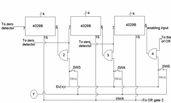
Figure 4. The Counter Unit
Display Unit
The display unit is made up of three 4511B integrated circuits as shown in the 7-segment decoder circuit of Figure 5. They are incorporated into the circuit to convert the BCD codes of the counters into corresponding 7-segment display. 220Ω resistors are connected to each segment lines to drop the voltage across corresponding LED segment.
For normal condition, the expected voltage at the segment or LED is 2.7V and current is 9.5mA [4][10].
Therefore, the voltage across the series resistor given by:
|
|
|
|
|
|
The resistor value used is 220Ω. This value is of more practical importance.
Pins 3 and 4 are made positive or at logical 1 while pin 5 is made low as specified by the datasheet of device [5].
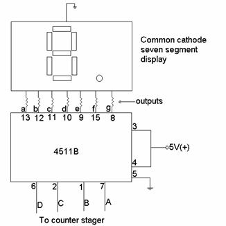
Figure 5. The circuit of a 7-segment decoder/display unit
Zero Detector
The zero detector is designed to indicate the “000” condition or reading of the counters. It is made up of a mere 3-input OR gate and an inverter. Its logic diagram is given in Figure 6.
The input of the OR gate is connected to the three carry-out outputs from the three counters in Figure 4. The output of the gate is low when all carry-output is low. Therefore, the inverter changes the low level logic to high. The zero detector is used for triggering the output through 4013B 3.
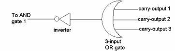
Figure 6. The zero Detector Unit
Output Unit
The output unit involves a relay switching circuit. It responds to signals from the control logic unit through 4013B 3 of Figure 3.
The output unit of Figure 7 has a NPN switching transistor (2SC945), a diode, and a 12V relay. The base of the transistor is connected to point m of 4013 B 3. Whenever terminal m is high, the transistor is switched on and the relay is energized and contact O2 is connected to O3. When the same terminal is low, the relay is de-energized and contact O2 is connected to O1.
The relay is a load of 400Ω. The circuit is connected to 12V power supply. The transistor has a typical current gain of 100 [5][11].
Therefore, the collector’s current is roughly
|
|
Therefore,
|
|
Therefore, the base resistor is given by:
|
|
|
|
10KΩ is the preferred value used for the design. The reverse biased diode at the relay is used to protect the transistor. It works against the Lenz’s law of induction in which there is an opposing voltage to voltage change in the coil. The diode cancels out the induced back-e.m.f. The e.m.f. produced due to switching can destroy the transistor. The diode is therefore used to protect the transistor.
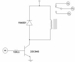
Figure 7. The Output Unit
Power Supply Unit
The circuit diagram of the dual power supply unit that was designed and used to power the entire circuitry of the programmable control timer is shown in Figure 8.

Figure 8. Power supply unit
Performance Evaluation
The normally open and close terminals of the relay were identified with the aid of a multimeter to avoid wrong connection of the relay contacts. The system was tested by connecting to it different loads with different time inputs to test its ability to switch it ON or OFF. Two loads were plugged to the system, one to the normally ON electric socket and the other to the normally OFF side. The system was then powered ON. Thereafter the set mode button was pressed. A particular time was SET through the three preset buttons and the set time indicated on the display. The countdown button was then pressed to activate counting down of the preset time. After a value of “000” was obtained on the seven-segment display (i.e. at zero-time mark) the two output electric sockets reversed their states, thereby making the electronic device which was ON to go OFF, and the other which was OFF to come ON. Different time values were set on the device during the test. The main aim of the test was to see the effect of zero-time mark on the output electric sockets. The results came out as expected.
Conclusion
A Simple Programmable Control Timer have been designed and constructed. The device uniqueness is in its ability to switch ON an initially OFF appliance and at the same time switch OFF another initially ON appliance connected to it after a preset time. The system is quite cheap, reliable and easy to operate.
References
1. Howstuffworks [online]; ©1998-2006 HowStuffWorks, Available at: http://www.howstuffworks.com/.
2. Morgan J., Time Management, Mood House Press, California, 1999.
3. Horowitz P., Hill W., The Art of Electronics, 2nd Ed., Cambridge University Press, New York, 2003.
4. Theraja B. L., Theraja A. K., A Textbook of Electrical Technology, Revised 23rd Ed, Chand Company Ltd, New Delhi, 2002.
5. Datasheet Search System [online]; ©2000-2006 Datasheet4u.com, Available at: http://www.datasheet4u.com
6. Ahmed M. S., Mohammed A. S., Onimole T. G., Attah P. O., Design and construction of a remote Controlled fan regulator, Leonardo Electronic Journal of Practices and Technologies, 2006, 9, p. 55-62 [online]. Available at: http://www.lejpt.academicdirect.org/A09/055_062.pdf
7. Mahmud S. A., Murtala B. Z. A., Kolo J.G., Design and Construction of a Remote Controlled Power Supply Unit, Leonardo Journal of Sciences, 2007, 11, p. 41-50 [online]. Available at: http://www.ljs.academicdirect.org/A11/041_050.pdf
8. Mahmud S. A., Abubakar S. M., Genesis A. A., Development of a Simple Sound Activated Burglar Alarm System, Leonardo Journal of Sciences, 2006, 9, p. 97-102 [online]. Available at http://www.ljs.academicdirect.org/A09/097_102.pdf
9. Forrest M. Mims III, Engineer’s Mini Notebook, Volume I. Timer, Op Amp & Optoelectronic Circuits & Projects, 1st Ed., Master Publishing, 1986.
10. Tocci R. J., Widmer N. S., Digital Systems: Principles and Applications, 7th Ed, Prentice-Hall International Inc, New Jersey, 1998.
11. Rizzoni G., Principles and Applications of Electrical Engineering, 3rd Ed., McGraw-Hill, New York, 2000.