Design of a Clap Activated Switch
Seyi Stephen OLOKEDE
Department of electrical & electronic engineering
College of engineering & technology
Olabisi onabanjo university,Ibogun,Ogun state
E-mail(s): solokede@yahoo.co.uk
+123 805 717 3799
Abstract
This paper presents the design of a clap activated switch device that will serve well in different phono-controlled applications, providing inexpensive key and at the same time flee from false triggering.
This involves the design of various sages consisting of the pickup transducer, low frequency, audio low power and low noise amplifier, timer, bistable and switches. It also consists of special network components to prevent false triggering and ensure desired performance objectives. A decade counter IC serves the bistable function instead of flip-flop, special transistor and edge triggering network for low audio frequency.
Keywords
Sound, multi vibrator, microphone, relay, triggering.
Introduction
The primary purpose of switch is to provide means for connecting two or more terminals in order to permit the flow of current across them, so as to allow for interaction between electrical components, and to easily isolate circuits so as to terminate this communication flow when need be. The motivating force behind this design is based on the desire to alleviate the problem faced by the aged and physically challenged persons in trying to control some household appliances. It also takes into considerations the illiterates that may have problems operating some “complex” hand-held Remote Control Units (RCUs)
Therefore this paper provides an introductory study on the basic principles involved in utilizing acoustic energy to control switching process. This is achieved by converting the energy generated by the “handclap” into electrical pulse, which is in turn used to drive an electronic circuitry that includes a relay [3], which in turn switches ON/OFF any appliance connected through it to the main.
The device is activated by clapping twice within a set time period that is determined by a time constant (RC) component value in the circuit [4].
Basic Design Elements
Clap Activated Switch
The clap activated switching device can basically be described as a low frequency sound pulse activated switch that is free from false triggering. The input component is a transducer that receives clap sound as input and converts it to electrical pulse. This pulse is amplified and used to drive IC components which changes output state to energize and also de-energize a relay causing the device to be able to switch larger devices and circuits. The output state of the switching device circuit can only change, when the circuit receives two claps within a time period that will be determined by the RC component value in the circuit.
The transducer (microphone) is connected to an amplifier sub-circuit which is connected to timer ICs [3]. These timer ICs are wired as monostable multi vibrators and their output is used to drive a decade counter IC that is wired as bi-stable to drive the relay.
The Transducer (Microphone) [8]
Microphones are types of transducers, they convert acoustic energy i.e. sound signal. Basically, a microphone is made up of a diaphragm, which is a thin piece of material that vibrates when it is struck by sound wave. This causes other components in the microphone to vibrate leading to variations in some electrical quantities thereby causing electrical current to be generated. The current generated in the microphone is the electrical pulse.
There are two major types of microphones based on the technical methods of converting sound into electricity namely the organic and condenser microphone. Table 1 shows the comparison between the dynamic and condenser microphone. Condenser microphones generally have flatter frequency responses than dynamic, and therefore mean that a condenser microphone is more desirable if accurate sound is a prime consideration as required in this design.
Mic Level and Line Level
The current generated by a microphone is very small and this current is referred to as mic level and typically measured in milli-volts. Before it is usable, the signal must be amplified, usually to line level, with typical value within (0.5 – 2) volts, which is stronger and more robust signal. The line level is the standard signal strength used by audio processing equipment [7]
Transistor
The bipolar NPN transistors used in this design are basically used as switch, to trigger the relay and as amplifier to boost the mic level to line level. When a transistor is used as switch, it must be either OFF or fully ON. In the fully ON state, the voltage VCE across the transistor is almost zero and the transistor is said to be saturated because it cannot pass any more collector current IC. The transistor is off when VIN is less than 0.7 V, because the base current will be zero. The power developed in a switching transistor is very small
In the OFF state
Power = VD *IC but IC = 0 (3.3.1)
P = 0
In the ON state
Power = VC * IC but VCE » O (almost) (3.3.2)
P » 0
So, the power is very small
Transistor as Amplifier
The basic action of the BC 549 transistor used for amplifier circuit in this design is to receive an input signal from the input transducer (microphone), control the amount of power that the amplifier takes from power source (Vs) and converts it into power needed to energize its load i.e. the 555 timer [2]. Generally, the collector current is controlled by the emitter or base current. By connecting a load effectively between the collector and the common terminal, the transistor can produce gain, and the input signal is generally an alternating quantity. However, the transistor requires operating in a unidirectional mode, otherwise, the negative parts of the alternating quantity would cause the emitter-base junction to be reverse biased and this would prevent normal transistor action. Consequently, it is necessary to introduce a bias. A transistor in the common-emitter circuit has the base-emitter junction forward biased and the collector-base junction reverse biased. Under these conditions and in the absence of an input signal
Ic = IB + Ic (3.3)
The leakage current is not necessarily negligible. The leakage is temperature dependent; hence an increase in temperature causes the leakage to rise. In turn, this result in collector current and a change in bias condition. The change in bias condition is therefore stabilized by using a potential divider R3 and R4 as shown in figure 1. The potential divider holds the base voltage almost constant.
The 555 Timer
The 555 timer is a very versatile 8-pin, which can be configured with a few external components and to build many circuits involving timing. The NE 555, used in this design is a popular version that is suitable in most cases where a 555 timer is needed. It is a dual-In -line (DIL) package.
The 555 timer configuration can be done in three modes but for the purpose of this design, two of them are required namely: astable and Monostable mode. An astable circuit produces a square wave with sharp transitions between low and high. It is called astable because it is not stable in any state since the output is continually changing between “low” and “high”.
A monostable circuit produces a single output pulse when triggered. It is stable in just one state; the “output low” state. This is also known as the triggered pulse producer. Once triggered by an input voltage, it gives a fixed length output pulse. It will do this for even short input pulse. The “output high” state is temporary. The duration of the pulse is called the time period (T), which is determined by resistor R8 and capacitor C3. The time period T, which is the time taken for the capacitor to change to 2/3 of the supply voltage is given as
T = 1.1 * R8 * C3 (3.4)
Relays
The relay is an electrically operated switch. If a small voltage is applied to its input terminal, it activates an electromagnet and closes its contacts. These contacts can then switch on larger amounts of current and voltage safely. But a low power transistor is also needed to switch the current for the relay’s coil.
Decade Counter
Counters are electronic circuits that count in binary and give outputs that changes every time an input signal changes from high to low (i.e. at every falling edge of the signal). A counter requires a square wave input signal to make it count. This wave is a digital waveform with sharp transition between low (0 V) and high
(+Vs), such as the output from a 555 timer circuit.
In this design, the output of a decade counter is used for a transistor switch that enables the switching of the relay. The decade counter, CD4017BC, used in this design is a 5 stage divide-by-10 counter with 10 decoded outputs and a carry out bit. Counters are cleared to their zero cont by a logical “1” on their reset line, and are advanced in their counts on the positive edge of the clock signal only when the clock enable is in the logical “0” state. The decade counter is a 16 pin Dual-in-Line (DIL) package. The decade counter IC CD4017B, used in this design is wired as a bistable, by connecting its decoded output “2” (Pin 4) to its reset (Pin 15).
The Design
The device is expected to control switching process by sensing hand claps, but must avoid being triggered by false signals, such as voice and mechanical noise impulse. The circuit is expected to respond to two claps only when it is received within three seconds to energize a relay which will make connection with an external circuit.
Design Calculations
For transistor Switch
Using general purpose transistor BC 548
Supply voltage, Vs = 9V
The load driven by the transistor is the relay Rl
Load resistance Rl = 150 ohm
Load current I1 = Supply Voltage, Vs
Load Resistance, Rl
= 9/150
= 60 mA
Since Il (max) must be greater than Il and from the date sheet Ic(max) = 100mA
Ic > Il
To calculate for Base Resistor, R2
![]() R2 =
Vc´hfe (4.2)
R2 =
Vc´hfe (4.2)
5´Ic
Where
Vc = Chip supply voltage
But since Vc = Vs
Then
![]() R14
= (Vs´hfe) (4.3)
R14
= (Vs´hfe) (4.3)
5´Ic
![]() = 9´400
= 9´400
5´100
= 7.2 KW
Where the typical hfe value = 400 from the date sheet, and Ic = 100 mA.
Therefore, R14 is selected to be 10 KW.
For light Emitting Diode (LED)
To determine the value of the voltage dropper resistor, the voltage supply value must be known. From this value, the characteristic voltage drop of an LED can then be subtracted, and the value of drop across an LED depending on the desired brightness and colour will range from 1.2 V to 3.0 V.
If(max) = 20mA
Vcc = 9V
Vf = 2V
Required current I(req) = 5mA.
![]() RLED
= Vcc–Vf (4.4)
RLED
= Vcc–Vf (4.4)
If (max)
![]() = 9-2
= 9-2
5´10-3
= 1.4 KW (4.5)
But choosing IR (LED) = 10mA
![]() R(LED)
= 9–2
R(LED)
= 9–2
10´10-3 (4.6)
= 0.7 KW
Where
VF = the maximum forward voltage drop
Vcc = the supply voltage
RLED = the LED current limiting resistor
Considering equations (4.5) and (4.6)
R9 and R13 are chosen to be 1KW
Design calculation for condenser microphone
From the data sheet, the electrets condenser microphone has the following specifications:
Rated Voltage = 2V
Operating Voltage = 1–10 V
Sensitivity = -44+/-3dB
S/N = 55dB
The microphone – biasing resistor, R1 is given by
![]() R1 = Vs–V(rated)
(4.7)
R1 = Vs–V(rated)
(4.7)
2mA
R1 = 3.5 KW
Therefore, R1 was chosen to be 3.3KW.
Design and calculation for IC1 (Monostable Multi vibrator)
The ON time (T) is the duration of the pulse and it is determined by the values of resistor and capacitor R8 and C3 respectively. The ON time (T) duration of the pulse is determined by the selected values of R8 and C3. Choosing C3 =10uF, since there are few available values: calculating for a time period of 3 seconds
T = 1.1´R8 ´C3 (4.8)
R8 = T/1.1´C3
= 3/10´10-6´1.1
= 273 KW
The nearest available resistor chosen as R8 = 270 KW
Design Calculation forIC2 (Monostable) with power on reset
To de-bounce the switch, IC1 (555 timer) is connected to make it trigger a 555 monostable circuit of IC2 with a very short time period (milli-seconds) and the output is used to drive the clock input of the counter.
Resistor R10 and capacitor C5 determines duration of the pulse and to prevent contact bounce
Choosing C5 = 0.01 µF
Calculating for a very short time of 1msec
T = 1.1´R10´C5 (4.9 )
R10 = T/ 1.1´C5
= 1´10-3/1.1´0.01´10-6
= 90.91 KW
Therefore selecting R10 = 100KW
To prevent false triggering
It is ensured that the monostable circuit of IC2 is reset automatically when power is supplied to it. This is achieved by a “Power ON” reset circuit. The capacitor C7 must take a short time to change, so as to briefly hold the input close to zero volts when the supply comes on resistor R11 of about 10 KW is usually used. R11 and C7 determine the duration for the brief delay before IC2 receives the triggering signal.
Chosen R11 = 10KW (Recommended)
Calculating for a time period of 24 milliseconds
T = 24msecs
R11 = 10´103
T = 1.1´R11´C7 (4.10)
C7 = T/1.1´R8
![]() = 24´10-3
= 24´10-3
1.1´10´103
C = 2.18 µF
Therefore, C7 is selected to be 2.2Uf
Design calculation for Transistor Amplifier
An audio low noise transistor is used for the audio signal amplifier circuit in this design, and this is wired in a common-emitter mode. At the saturation level, maximum collector current for an emitter-base design can be determined by applying a short circuit between the collector-emitter terminals. At this point, the voltage across the collector-emitter junction is almost zero.
From data sheet, Vce(sat) = 0.3 V
Ic (sat) = Vs-Vce (sat) (4.12)
Rc + RE
Where Ic = 2mA
2mA=9–0.3
Rc+RE
Rc +RE=9 – 0.3/ 2´10-3
=4.34KW
For linear amplification and maximum output purpose, the operating point should lie around the dc load-line. The quiescent point normally takes a value of about half the supply voltage.
The quiescent, Vce = 9/2 (4.13)
= 4.5 V
the emitter terminal is made to be a little above ground level. Therefore, voltage from emitter to ground, VE is usually arranged to be one tenth of supply voltage, VS.
VE = VS/10 (4.14)
= 9.0/ 10
= 0.9 V
Hence the emitter resistor
R6 = VE/IE 4.15)
R6 = VE /IE
= VE/ IC
= 0.9/2´10-3
= 450 W
The voltage drop across R4 is given by
VB = R4/ R3+R4´VS (4.16)
IB–IBRTH – VBE – IERE=0 (4.17)
Substituting IE = (b + 1) IB into equation 4.17, we have
IB–IBRTH–VBE-(b+1) IBRE=0
IB=VB–VBE/ [RTH+ (b+1) RE] 4.18)
VB = VE–VBE (4.19)
= 0.9 – 0.7
= 0.2 V
From equation 4.16, we have
VB(R1 +R4)=R2VCC (4.20)
0.2 (R1+R4) =9R2
0.2R1 + 0.2R4 = 9R4
R1 = 44R4 (4.21)
And 10R4£bRE
Where RE=450 W and
b=650
From data sheet
R4 £650´450 /10
=29,250W
hence R4 = 30 KW
then, from equation 4.21, we have
R3=44´40 KW
=1320 KW
=1.3 MW
VCE = 4.5V from equation 4.13
Then
RS + RE = Vs – VCE / IC
=9.0 – 4.5 / 2´10-3
RS + RE = 2.25 KW
RE=2.25 KW – 450 W
=1.75 KW
Testing
The individual component circuits were delineated in the design and tested to satisfy the operational purpose and desired performance, especially those of the timing circuits. The monostable circuit of IC2 of the complete circuit diagram was by-passed. It was observed that at a single clap, the relay made several clicking noise. It was inferred that the vibrating effect of the relay is as a result of the bounce of the switch fired by several pulses generated from the decade counter. Therefore it is of significant importance to de-bounce the switch using the combination of “Power-ON Trigger” and “Power-ON Reset” circuits. Using a single 555 timers and by-passing IC1 in the original circuit it was observed that the red LED, indicating the time period only flashed once at a single clap and the relay was energized, but there was no bounce noticed. For edge-triggering test, the resistor R is removed, and it was observed that the indicator LED1 became permanently ON and the circuit did not respond to further inputs (claps), and could not energize the relay. If the trigger input was still less than Vs/3 at the end of the time period, the output will remain high until the trigger is greater than Vs/3. The situation occurred since the input was from a microphone (sensor)
The circuit was placed on a hard table surface, and the surface was struck twice within the design set “Time Period”. It was observed that the indicator LED1 became ON for the stricken several times, but the normal time duration, but relay was also stricken several times, but same result was observed. The vibration test was repeated, but with the microphone allowed to make contact with the table surface. It was observed that the circuit responded and the relay was energized. For interference due to vibration effect, the microphone surface should be padded to prevent it from making direct contact with the casing, so as to avoid mechanical vibration being transmitted to the mic through the casing of the casing of this casing of this device. Also, the circuit board will be installed on standoffs in the base of case. The standoffs may be needed to provide support in areas of high potential mechanical stress on the circuit board, like the area where doors are slammed especially if this device is installed on susceptible wall close to the door. The rating of this device is as important as the device itself, since the loading capacity can influence performance and functionality of switches. Light bulbs were used to test for the maximum load limit which this “clap activated switching device” can be use to switch comfortably. The result of the wattage test is presented in Table 1
Conclusion
The clap activated switching device function properly by responding to both hand claps at about three to four meter away and finger tap sound at very close range, since both are low frequency sounds and produce the same pulse wave features. The resulting device is realizable, has good reliability and it’s relatively inexpensive.
Acknowledgements
The author wish to acknowledge the kind cooperation of the laboratory technologies of the Department of Electrical & Electronic Engineering, of the Olabisi Onabanjo University, Ibogun, Ogun State, Nigeria.
Table1: Comparison Between Dynamic And Condenser Microphone
|
Dynamic Microphone |
Condenser Microphone |
|
Do not have flat frequency response but rather tend to have tailed frequency response for particular applications |
Have a flat frequency response |
|
Operate with the principle of Electromagnetism as it does not require voltage supply. |
Employs the principle of electrostatics and consequently, require voltage supply across the capacitor for it to work. |
|
They are suitable for handling high volume level, such as from certain musical instruments. |
They are not ideal for high volume work as their sensitivity makes them prone to distortion. |
|
The signal produced are strong therefore making them sensitive |
The resulting audio signal is stronger than that from a dynamic. It also tends to be more sensitive and responsive than dynamic. |
Table 2:Load And Wattage Calibration Exercise Result.
|
S/N |
Test description |
Watts |
Observation |
|
1 |
Lightning bulb connected across device |
60 |
Device switched accurately |
|
2 |
Fluorescent connected across device |
100 |
Device switched accurately |
|
3 |
A CD cassette player tape recorder connected across device |
150 |
Device switched accurately |
|
4 |
Combination of light bulb and tape player connected across device |
150+60 |
Device switched comfortably |
|
5 |
Combination of light bulbs |
300 |
Device switched comfortably |
|
6 |
Combination of light bulbs |
460 |
Switched but bounced several times |
|
7 |
Vacuum cleaner connected across device |
1200 |
Switch with bounces but failed after. |
|
8 |
Television set connected across device |
|
Device switched comfortably. |
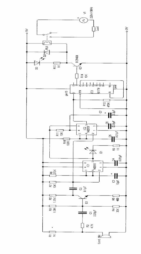
Figure 1:Circuit Diagram Of A Clap Activated Switching Device
References
1. Edward Hughes, Hughes Electrical technology, Addition Wesley Longman (Singapore) plc Ltd, India, Seventh Edition, pp 395-399, 2001.
2. Paul Horonitz and Weinbeild Hill, the Art of Electronics, second Edition, Cambridge University Ulc, 1995.
3. Ray Marston, “Relay Output Circuits”, Electronics Now Magazine, July 1994.
4. http://www.kpsec.com: Country circuits, the Electronics club
5. Alex Pounds, “Electronics Tutorial” Denenberg University,
http://www.ffldusoe.edu/faculty/Denenberg/topics/Electronics/AlexPounds.htmls. Retrieved May 5, 2007.
http://www/the 12volt.com.SPDT automobile Relays, 2004
6. http://www/starmicromics .com/components/mics.html: Microphone series
7. The Audio Forum “How Microphones Work”, www.mediccollege.com
8. Tony Van Roon (VA3AVR) “Relays and Relay Drivers” www.starcounter.com
December 6, 2006.
9. The Electronics Clubs, “Transistor Circuit”, www.kspec.com
www.mccsemi.com. NPN Silicon Amplifier Transistor