Chemical Bath Deposition of Nickel Sulphide (Ni4S3) Thin Films
Kassim ANUAR1, Nagalingam SARAVANAN2, WeeTee TAN1, SoonMin HO1 and Darren TEO1
E-mail: anuar@science.upm.edu.my
Abstract
Thin films of nickel sulphide were deposited from aqueous baths on indium tin oxide glass substrate. The chemical bath contained nickel sulphate, sodium thiosulfate and triethanolamine solutions. The aim of the present study was to analyze the different experimental conditions to prepare Ni4S3 thin films using chemical bath deposition technique. The structural, morphological and optical properties of nickel sulphide thin films were obtained by X-ray diffraction, atomic force microscopy and UV-Vis Spectrophotometer will be presented. The properties of the films varied with the variation in the deposition parameters. The films deposited at longer deposition time using lower concentration in more acidic medium showed improved crystallinity, good uniformity and better adhesion to the substrate. Films showed band gap of 0.35 eV and exhibited p-type semiconductor behaviour.
Keywords
Chemical bath deposition; Thin Films; Nickel Sulphide; Semiconductor.
Introduction
There has been a growing interest in the binary compounds because of their electronic and optical applications. Nickel sulphide thin films belong to VIII-VI compound semiconductor materials. They have a number of applications in various devices such as solar cells, sensors, photoconductors and infrared detectors. A variety of methods, including electrodeposition [1], SILAR [2], pulsed laser ablation [3], metal-organic chemical vapour deposition [4], thermal and photochemical chemical vapour deposition [5] can be used for the preparation of nickel sulphide thin films. Chemical bath deposition method is an attractive choice due to its simplicity, low cost, low temperature and potential for large-scale production. Up-to-date, chemical bath deposition method has been successfully used to deposit many different semiconductors thin films including CdS [6] Sb2S3 [7] and CdSe [8], Cu4SnS4 [9] and ZnxCd1-xS [10]. So far, there is no report on deposition of Ni4S3 thin films from aqueous solution using triethanolamine as complexion agent at room temperature by chemical bath deposition method.
In this study, Ni4S3 thin films were produced using chemical bath deposition method. Triethanolamine was used as complexing agent. The influences of deposition parameters, including deposition time, pH and solution concentration on the properties of thin films were studied. The results of the investigation on structural, morphological and optical properties of thin films have been carried out by using X-ray diffraction, atomic force microscopy and UV-Vis Spectrophotometer technique, respectively.
Material and Method
Preparation of thin films
All the chemicals used for the deposition were analytical grade and all the solutions were prepared in deionised water (Alpha-Q Millipore). The nickel sulphide thin films were prepared from aqueous solutions of nickel sulphate (NiSO4) and sodium thiosulfate (Na2S2O3.5H2O) acted as a source of Ni2+ and S2- ions, respectively. Triethanolamine (TEA) was used as complexing agent during deposition. The indium-doped tin oxide (ITO) glass substrates were used as the substrate for the chemical bath deposition of nickel sulphide thin films. Before deposition, the glass substrates were degreased with ethanol for 10 min. Then, ultrasonically cleaned with distilled water for another 10 min and dried in desiccators. Deposition of thin films was carried out at room temperature in the following manner. 25 mL of NiSO4 was taken in a 100 mL beaker and 5mL of concentrated TEA was mixed in it. Subsequently, 25 mL of Na2S2O3 was added in it with constant stirring. The cleaned glass substrate was immersed vertically into beaker. The deposition was carried out at different pH values (pH 2.5 and 3), deposition times (1 and 3 hours) and solution concentrations (0.075 M and 0.1 M) in order to determine the best conditions for the deposition of thin films. After the completion of deposition, the films were washed with distilled water and kept for analysis.
Characterization of thin films
The structure of the film was monitored by X-ray diffraction (XRD) with a Philips PM 11730 diffractometer equipped with a CuKα (λ=0.15418 nm) radiation source. Data were collected by step scanning from 25° to 60° with a step size of 0.05° (2θ). Surface morphologies of the films were observed by using a Q-Scope 250 (Quesant Instrument Corporation) atomic force microscope in a contact mode. Photoelectrochemical experiments were performed in [Fe(CN)6]3-/[Fe(CN)6]4- redox system, by running linear sweep voltammetry between +1 to -1 V versus Ag/AgCl. The halogen lamp (100 W) was used for illuminating the electrode. The optical properties of the film were measured with a Perkin Elmer UV/Vis Lambda 20 Spectrophotometer. The data were registered from 300 to 800 nm with an uncoated glass as a reference. The absorption data were manipulated for the determination of the band gap energy.
Discussion of Results
Figure 1 shows the XRD patterns of nickel sulphide thin films grown at pH 2.5 for 3 hours under different solution concentrations. The observed peaks at 2θ = 30.2°, 50.3° and 59.5° positions correspond to the (111), (220) and (311) planes. The comparison of the observed diffraction peaks with the standard (JCPDS Reference code: 00-052-1027) confirmed that the material is the cubic of nickel sulphide [11]. Comparison between the films deposited at 0.075 M and 0.1 M reveals that the intensity of the peaks increased, indicating better crystalline phase in the films prepared at lower concentration. This could be clearly seen in the peak attributable to (111) plane, which is more intense. On the other hand, the peaks marked “◊” in the Figure 1 at 2θ =35.4° and 45.2° are belong to indium tin oxide [12] (JCPDS Reference code: 01-089-4597). These peaks are come from ITO glass used as substrate during deposition process.
Figure 2 shows the surface morphology of Ni4S3 thin films (5μm x 5 μm) deposited on ITO glass substrates. The atomic force microscopy results suggested that the influence of solution concentrations on the surface morphology is significant. The films prepared at lower concentration (0.075 M) reveal smooth surface with small grain size and high degree of homogeneity as compared with higher concentration. The surface morphology of Ni4S3 thin films prepared using higher concentration of nickel sulphate and sodium thiosulfate shows non-uniform grain size. The grains were distributed randomly over the surface of substrate. The sizes of the grains exhibit random orientation as it varies from one to each other. The thickness recorded for the films deposited at 0.075 M and 0.1 M is 37 and 53 nm, respectively.
The absorbance spectra of Ni4S3 thin films deposited at different solution concentrations are shown in Figure 3. With the increasing wavelength of radiation, the absorbance of all samples tended to be lowered. In the case of the films deposited using 0.075 M, the absorbance of the films is found to be better compared to that of the films prepared using 0.1 M of nickel sulphate and sodium thiosulfate. This is due to the grains were distributed randomly over the surface of substrate at higher solution concentration.
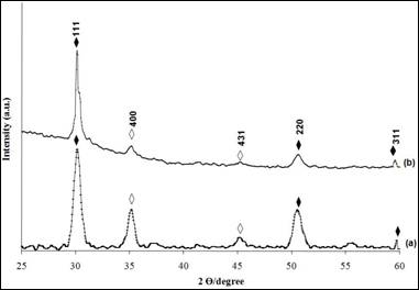
Figure 1. The X-ray diffraction patterns for Ni4S3 thin films deposited at various solution concentrations. (a) 0.075 M (b) 0.1 M (Experimental conditions: pH=2.5, time =3 hours)
(♦Ni4S3; ◊In1.875O3Sn0.125 )
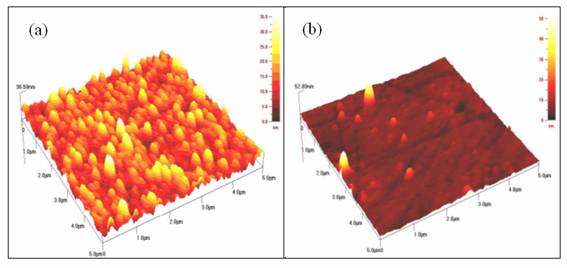
Figure 2. The atomic force microscopy images for Ni4S3 thin films deposited at various solution concentrations. (a) 0.075 M (b) 0.1 M
(Experimental conditions: pH=2.5, time =3 hours)
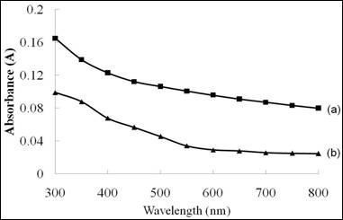
Figure 3. The absorbance versus wavelength spectra of Ni4S3 thin films deposited at various solution concentrations. (a) 0.075 M (b) 0.1 M
(Experimental conditions: pH=2.5, time =3 hours)
The XRD patterns of the deposited nickel sulphide thin films at pH 2.5 using 0.075 M of solution concentration under different deposition times are shown in Figure 4. The peaks obtained point out that Ni4S3 structure with (111), (220) and (311) planes have been deposited. When the deposition time is increased from 1 to 3 hours, the intensity of all the peaks is increased. Diffraction along the (111) plane shows the highest intensity with well-defined sharp peaks indicating high crystallinity of the material prepared.
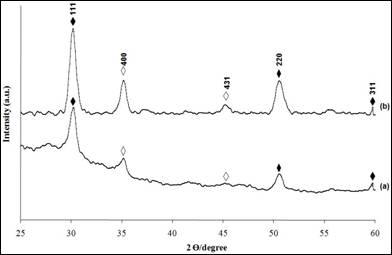
Figure 4. The X-ray diffraction patterns for Ni4S3 thin films deposited at various deposition times. (a) 1 h (b) 3 h (Experimental conditions: pH=2.5, solution concentration =0.075 M)
(♦Ni4S3; ◊In1.875O3Sn0.125 )
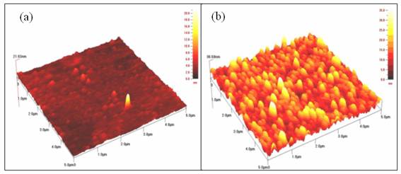
Figure 5. The atomic force microscopy images for Ni4S3 thin films deposited at various deposition times. (a) 1 h (b) 3 h
(Experimental conditions: pH=2.5, solution concentration =0.075 M)
The influence of deposition time on surface morphology of nickel sulphide thin films is shown in Figure 5 as revealed by AFM images. The films deposited at 1 hour show low appearance of grains over the film surface. However, there seems an increase in the number of grains for the films prepared at 3 h. These films also exhibit better morphology and larger grain size compared to the films deposited at shorter time. The film thickness is observed to increase (22 to 37 nm) with an increase in deposition time. In the chemical bathy deposition process, the film thickness increases with longer deposition time due to the film formation.
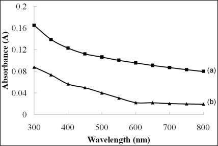
Figure 6. The absorbance versus wavelength spectra of Ni4S3 thin films deposited at various deposition times. (a) 3 h (b) 1 h
(Experimental conditions: pH=2.5, solution concentration =0.075 M)
Figure 6 shows the optical absorbance spectra for the Ni4S3 thin films deposited at various deposition times. It is clear that the thicker films (3 hours) possess higher absorption compared to the films deposited at 1 hour. This could be due to more Ni4S3 thin films deposited onto the surface of substrate providing better absorption properties.
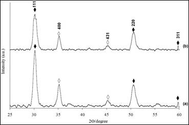
Figure 7. The X-ray diffraction patterns for Ni4S3 thin films deposited at various pH values. (a) pH 2.5 (b) pH 3 (Experimental conditions: time=3 h, solution concentration =0.075 M)
(♦Ni4S3;◊In1.875O3Sn0.125 )
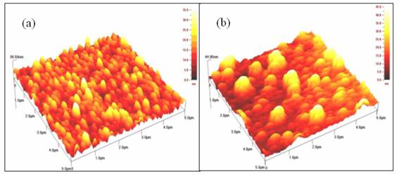
Figure 8. The atomic force microscopy images for Ni4S3 thin films deposited at various pH values. (a) pH 2.5 (b) pH 3
(Experimental conditions: time=3h, solution concentration =0.075 M)
The XRD patterns of thin films deposited at 3 hours using 0.075 M of solution concentration under different pH values were recorded as shown in Figure 7. The intensity of (111) plane is the highest appearing at 2θ=30.2° for all samples. Other minor peaks at 2θ = 50.3° and 59.5° belong to (220) and (311) planes, respectively.
Surface morphology of the films was studied with the help of AFM. Figure 8 shows the AFM images for the films deposited at various pH values. The AFM image shows that the films deposited at pH 2.5 are very dense and the grains are well crystallized. At pH 3, the films are composed of largely irregular-shaped grains of diameter 0.4-0.5 μm. The thickness of the films was measured using AFM technique. The obtained results show that there is an increase in thickness (37 to 45 nm) with an increase in pH value.
Figure 9 shows the absorbance spectra of Ni4S3 thin films prepared at different pH values. The films prepared at pH 2.5 showed higher absorption characteristics when compared to the films deposited at pH 3. This is due to uniform and continuous distributions of grains with large surface area were obtained under this experimental condition.
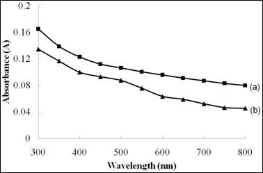
Figure 9. The absorbance versus wavelength spectra of Ni4S3 thin films deposited at various pH values. (a) pH 2.5 (b) pH 3
(Experimental conditions: time=3h, solution concentration =0.075 M)
In order to determine the band gap of thin films, the equation of Stern [13] was used.
![]() (1)
(1)
where n is the frequency, h is the Planck’s constant, k equals a constant while n carries the value of either 1 or 4. The n value is 1 for a direct gap material and 4 for indirect gap material. From the Figure 10, the value of band gap was estimated by extrapolation of the straight-line in the plot of (Ahn)2 versus the photon energy. The band gap energy of grown films in optimized conditions (time=3h, solution concentration =0.075 M, pH=2.5) is 0.35 eV. The similar band gap energy has also been reported by other researchers for deposition of nickel sulphide films using SILAR method [14].
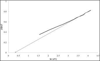
Figure 10. Plot of (Ahn)2 versus hn band gap for Ni4S3 thin films prepared under optimized conditions. (Experimental conditions: time=3h, solution concentration =0.075 M, pH=2.5)
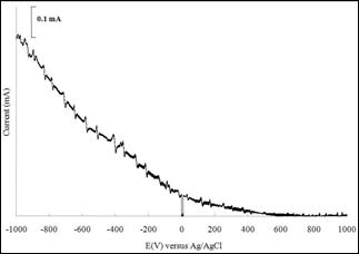
Figure 11. Photoresponse for Ni4S3 thin films prepared under optimized conditions. (Experimental conditions: time=3h, solution concentration =0.075 M, pH=2.5)
The photoresponse of nickel sulphide thin films is investigated when lights were shone and chopped at an almost constant frequency during the photoelectrochemical test. Figure 11 shows the photoresponse of the Ni4S3 thin films prepared under optimized conditions (time=3h, solution concentration =0.075 M, pH=2.5) in contact with [Fe(CN)6]3-/[Fe(CN)6]4- redox system solution. The current change shows semiconductor behaviour of the materials. When the sample was illuminated, the current increases while the current flow decreases as the light was interrupted by chopping process. Significantly, the photocurrent occurs on negative potential shows the films prepared are of p-type material. Sartale and Lokhande [2] have also reported similar type of semiconductor for nickel sulphide thin films prepared using SILAR method.
Conclusions
Thin films of nickel sulphide have been synthesized using chemical bath deposition method. The XRD patterns showed the films were polycrystalline in nature with cubic phase and exhibited preferentially along the (111) direction. It was observed that the deposition parameters could significantly change the crystallinity and morphology of the films. At lower pH, the crystallinity of the films was improved. The films prepared using lower concentration at longer time showed smooth surface with small grain size and high degree of homogeneity based on AFM images. According to XRD, AFM and UV-Visible results, the best quality of Ni4S3 thin films have been grown on indium tin oxide glass substrate at pH 2.5 using 0.075 M of nickel sulphate and sodium thiosulfate for 3 hours.
Acknowledgements
The authors would like to thank the Department of Chemistry, Universiti Putra Malaysia for the provision of laboratory facilities and to MOSTI for the National Science Fellowship.
References
1. Anuar K., Zulkarnain Z., Saravanan N., Zuriyatina A., Sharin R., Preparation and studies of nickel sulfide thin films in the presence of sodium tartrate as a complexing agent, Materials Science (Medziagotyra), 2004, 10, p. 157-161.
2. Sartale S.D., Lokhande C.D., Preparation and characterization of nickel sulphide thin films using successive ionic layer adsorption and reaction (SILAR) method, Materials Chemistry and Physics, 2001, 72, p. 101-104.
3. Lee H.Y., Kanai M., Kawai T., Kawai S., Growth of oriented NiS films on Si(111) and Al2O3(012) substrate by pulsed laser ablation, Japan Journal of Applied Physics, 1993, 32, p. 2100-2101.
4. Nomura R., Hayata H., Growth of transition metal sulfide thin films from dithiocarbamate complexes by MOCVD technique, Transactions of the Materials Research Society of Japan, 2001, 26, p. 1283-1286.
5. Cheon J.W., Talaga D.S., Zink J.I., Laser and thermal vapour deposition of metal sulfide (NiS, PdS) films and in situ gas-phase luminescence of photofragments from M(S2COCHMe2)2, Chemistry of Materials, 1997, 9, p. 1208-1212.
6. Karimi M., Rabiee M., Moztarzadeh F., Tahriri M., Bodaghi M., Controlled synthesis, characterization and optical properties of CdS nanocrystalline thin films via chemical bath deposition (CBD) route, Current Applied Physics, 2009, 9, p. 1263-1268.
7. Krishnan B., Arato A., Cardenas E., Roy T.K.D., Castillo G.A., On the structure, morphology and optical properties of chemical bath deposited Sb2S3 thin films, Applied Surface Science, 2008, 254, p. 3200-3206.
8. Esparza-Ponce H.E., Hernandez-Borja J., Reyes-Rojas A., Cervantes-Sanchez M., Vorobjev Y.V., Ramirez-Bon R., Perez-Robles J.F., Growth technology, X-ray and optical properties of CdSe thin films, Materials Chemistry and Physics, 2009, 113, p. 824-828.
9. Anuar K., Tan W.T., Atan M.S., Dzulkefly K.A., Jelas M.H., Ho S.M., Saravanan N., Preparation and characterization of chemically deposited Cu4SnS4 thin films, Journal of Ultra Chemistry, 2009, 5, p. 21-26.
10. Song W.C., Lee J.H., Growth and characterization of ZnxCd1-xS films prepared by using chemical bath deposition for photovoltaic devices, Journal of Korean Physical Society, 2009, 54, p. 1660-1665,.
11. Kitakaze A., Sugaki A., Study of the Ni3+xS2 phase in the Ni-S system with emphasis on the phases of high-form Ni3S2 (β1) and Ni4S3 (β2), Neues Jahrbuch Mineralogie Monatshefte, 2001, 41-48,.
12. Nadaud N., Lequeux N., Nanot M., Jove J., Roisnel T., Structural studies of tin-doped indium oxide (ITO) and In4Sn3O12, Journal of Solid State Chemistry, 1998, 135, p. 140-148.
13. Stern F., Elementary theory of the optical properties of solids, Solid State Physics, 1963, 15, p. 299-408.
14. Pathan H.M., Lokhande C.D., Deposition of metal chalcogenide thin films by successive ionic layer adsorption and reaction (SILAR) method, Bulletin of Materials Science, 2004, 27, p. 85-111.