Comparison of Steady State Electron Transport
Properties in Binary Nitride Materials Using
Hadi ARABSHAHI1*, Elham JABERI2, and Hossain TAYARANI2
1Physics Department,
2Physics Department, Khayyam
Institute of Higher Education,
E-mail: hadi_arabshahi@yahoo.com
* Corresponding author: +98 (512) 6223037
Abstract
An ensemble
Keywords
Ensemble
Introduction
In recent years,
III-Nitride semiconductors including compounds such as GaN,
AlN,
Different numerical methods can be used for calculating properties of electron transport in semiconductors and parts which of made them such as relaxation-time approximation, iterative method to solve the Boltzmann equation and Matthiessen's rule [4].
In this article, we study electron
transport in wurtzite GaN, AlN, and
Material and Method
In this work, a three valley model for the conduction band is employed.
Non-parabolicity is considered in all valleys. The
scattering mechanisms are ionized impurity, polar optical phonon, piezoelectric
and acoustic deformation potential. Elastic ionized impurity scattering is
described using the screened Coulomb potential of the Brooks-Herring model. In each
simulation, the motion of 3000 electrons is considered, and the initial
electron distribution is set according to equilibrium Fermi–Dirac
statistics. Throughout this study, we focus on the wurtzite
phases of GaN, AlN and
Table 1. Material parameter selections for wurtzite GaN,
|
|
GaN |
AlN |
|
|
Mass density (g/cm3) |
6.15 |
3.23 |
6.81 |
|
Sound velocity (m/s) |
6560 |
9060 |
6240 |
|
Acoustic deformation potential |
8.3 |
9.5 |
7.1 |
|
Static dielectric constant |
9.5 |
8.5 |
15.3 |
|
High frequency dielectric constant |
5.35 |
4.77 |
8.4 |
|
Effective mass (Г valley) |
0.2 |
0.31 |
0.11 |
|
Direct energy gap (eV) |
3.5 |
6.2 |
2 |
Table 2. Valley parameter selections for wurtzite GaN,
|
|
GaN |
AlN |
|
|
m*Г |
0.2 |
0.31 |
0.11 |
|
m*U |
0.4 |
0.39 |
0.4 |
|
m*K |
0.3 |
0.54 |
0.3 |
|
α Г |
0.189 |
0.32 |
0.419 |
|
α U |
0.065 |
0.5 |
0.065 |
|
α K |
0.7 |
0.03 |
0.7 |
|
Г - U |
2 |
0.61 |
1.9 |
|
Г - K |
3.1 |
0.67 |
2.63 |
Degeneracy effects are
expected to be negligible over almost all of the temperature and electron concentration
ranges of interest here and, hence, are not considered in the calculation.
Electron particles in the ensemble
Results
The bulk group III-Nitride velocity-field characteristics, predicted by our model are shown in Fig 1. For all cases, the temperature is 300 K and the donor concentration is 1023 m-3. We see that each compound exhibits a peak in its velocity-field characteristic. The peak drift velocity for InN is around 4.15×10⁵ ms-1, while those for GaN and AlN are about 3.08×10⁵ ms-1 and 2.17×10⁵ ms-1, respectively. At higher electric fields the drift velocity decreases, eventually saturating at around 2.03×10⁵ ms-1 for both GaN and AlN and 1.8×10⁵ ms-1 for InN [7-8].
The threshold fiels are 1.74×10⁷ Vm-1 and
2.79×10⁷
Vm-1 for GaN and AlN,
respectively. For
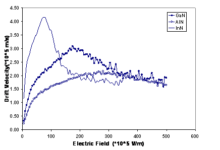
Figure 1. Calculated electron steady-state drift
velocity in bulk
as a function of applied electric field. The donor concentration is set to 1023 m-3 and temperature to 300 K.
The valley occupancies for Г, U and K are illustrated in figure 2
and show that the inclusion of the satellite valleys in the simulation is important.
Significant intervalley scattering into the satellite
valleys occurs for fields above the threshold field for each material. This is
important because electrons which are near a valley minimum have small kinetic
energies and are therefore strongly scattered. It is apparent that intervalley transfer is substantially larger in
In the figure we can also see that the behaviour of AlN is different from other semiconductors, because of having small energy gap between the Г valley and the other valleys and large effective mass of Г valley. At the field corresponding to the peak velocity in AlN, we find occupancies of 8% and 2% for the U and K valleys, respectively.
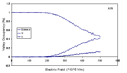
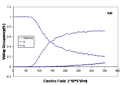
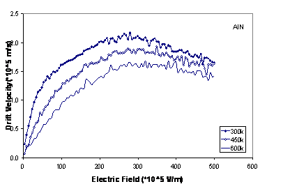
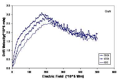
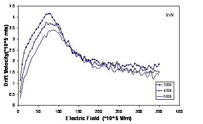
In figure 3, we plot the Г valley occupancies in each material as a function of Electric field at various temperatures. The total scattering rate of electrons increases, when the temperature increases and energy of electrons decreases due to collisions. Therefore, the number of electrons increases in central valley and decreases in Adjacent valleys.
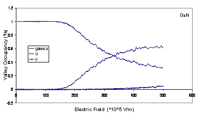
Figure
2.
Comparison of the valley occupancies as a function of electric field in bulk wurtzite GaN, AlN
and
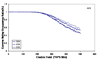
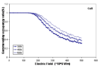
Figure 3. The Г valley occupancies in wurtzite AlN and GaN at 300, 450 and 600 K
In figure 4, we have plotted the drift velocity in each material as a function of Electric field at various temperatures. With increasing temperature, we can see a decrease in drift velocity at electric fields lower than threshold field, because of increasing intravalley scattering rate (scattering due to the acoustic phonon, ionized impurity, piezoelectric). The decrease in velocity at higher fields is due to increased intervalley scatterings. It is clear that increasing temperature, there are decreasing in the peak of drift velocity and shifting to higher electric field.
For
Figure
4. The drift velocity in wurtzite GaN, AlN
and
Conclusions
The computed steady-state and transient
electron transport in wurtzite GaN,
AlN and
We have shown that steady-state drift velocity in GaN is greater than others. So, it suggested for making the high frequency electronic devices.
The peak of drift velocity in
References
1. Arabshahi H., Comparison of SiC and ZnO Field Effect Transistors for High Power Applications, Modern Physics Letters B, 2006, 20, p.787-793.
2. Arabshahi H., Calculation of Electron Hall Mobility in GaSb, GaAs and GaN Using an Iterative Method, African Physical Review, 2007, p. 45-51.
3. Arabshahi H., The Effect of Polaron Scattering Mechanisms in Electron Transport Properties in Semiconductor Devices, International Journal of Science and Advanced Technology, 2012, 2(2), p. 84-86.
4. Turner G.W., Eglash S.J., Strauss A.J., Comparison of High Field Staedy State and Transient Electron Transport in Wurtzite GaN, AlN and InN, J. Vac. Sci. Technol. B, 1993, 11, p. 864-870.
5. Maslar J.E., Wang C.A., The Effect of Strain Rate Variations on the Microstructure and Hot Deformation Behaviour of AA2024 Aluminium Alloy, Appl. Spectrosc., 2007, 61, p.1093-1098.
6. Bennett H., Heckert A., Calculation of Electron Hall Mobility in GaSb, GaAs and GaN Using an Iterative Method, J. Appl. Phys., 2005, 98, p. 103705-103709.
7. Meyer J, Ram-Mohan L.R., Comparison of Steady-State and Transient Electron Transport in InAs, InP and GaAs, Appl. Lett., 1995, 67, p. 2756-2762.
8. Arabshahi H., The Frequency Response and Effect of Trap Parameters on The Charactersitics of GaN MESFETs, The Journal of Damghan University of Basic Sciences, 2007, 1, p. 45-49.