Fabrication and characteristics of Hg/n-bulk GaN schottky diode
Belkadi NABIL1, Rabehi ABDELAZIZ2, Zahir OUENNOUGHI1, Abdelmalek DOUARA2
1Department of Phyisics, Farhet Abbas University, Setif, Algeria.
2Laboratoire de Microélectronique Appliquée, Université Djillali Liabés,B. P. 89, 2200 Sidi-Bel-Abbès, Algérie.
E-mails: bel.nabil@yahoo.fr, rab_ehi@hotmail.fr
Abstract
In this work, the electrical characteristics of bulk gallium nitride doped n have been investigated by the current–voltage (I–V) and capacitance-voltage (C-V) at 300 K temperature. Using the thermionic emission theory, the saturation current, IS (2.45×10⁻⁷ A), the ideality factor n (1.13), the barrier height ϕbn (0.65) and the serial resistance RS (670) are determined for our structure (Hg/n-GaN). It has also been calculated the barrier height from C–V experimental data. The determined value is higher (1.24 eV) compared with the value obtained from I–V (0.65 eV) characteristics, it was found the following electrical parameters, doping concentration (ND = 1.68×1016 cm-3, diffusion voltage (Vd = 1.11 V) and density of interface states (Nss).
Keywords
Electrical Characteristics; Bulk GaN; Shottky; Diode, Barrier; Height; Density of Interface States
Introduction
GaN is the most popular material in this field of research. These electrical, electronic and mechanical properties make him the best candidate in the field of high frequency power electronics and optoelectronics [1-3]. Various studies have shown that devices made of GaN exhibit better performance than those based on conventional semiconductors although the GaN contains a high density of defects produced during its development.
To reduce the density of defect layers in GaN, studies are being undertaken to look for the best technique to develop a defect-free GaN.
The latest guidance is that which consists in the bulk GaN. Some have resulted in obtaining bulk GaN but improvements are needed to optimize and monetize the different techniques. Some parameters of Schottky diode such as barrier height, doping concentration and diffusion potential can be derived from C−2 (V) relationship [4, 5]
The purpose of this paper is to realize and characterize Schottky diodes based on bulk GaN, there have been investigated the different electrical parameters determined from (I-V) and (C-V) characteristics of the Hg /n-GaN structure. From the forward bias current–voltage (I–V) characteristics, we have determined the saturation current (Is), the ideality factor (n), the Schottky barrier height (φbn) and the series resistance (Rs). Capacitance-voltage (C-V) measurements also have given detailed information about Schottky contacts.
Material and method
The bulk GaN is used as an n-type unintentionally doped Lumilog, the growth technique used is the HVPE (Hybrid Vapor Phase Epitaxy) freestanding GaN.
Deposition of ohmic contact is on the rear side using the coating of silver (Ag) and the Schottky contact deposited sue the front face is a temporary drop Mercury (Hg), the surface is 1 mm in diameter.
The following figure illustrates the pattern of the sample obtained after the deposition of Ohmic contacts and Schottky (see Figure 1).

Figure 1. Schottky diode made on n-type bulk GaN with temporary Mercury contact
The I–V measurement was investigated using a conventional method. The electrical current was measured using a HP4155B instrument at room temperature and in the dark.
The C–V measurement was obtained using a KEITHLEY test system 590 CV Analyser, by applying a DC between −4 V and 0 V with 1 MHz frequency, so that the interface states are unable to the respond to the AC signal.
Table 1. Classic parameters of GaN at 300 k [6]
|
Parameters |
Values (units of measurements) |
|
Effective density of electrons in the conduction band (Nc) |
2.6×1018 cm-3 |
|
Effective density of electrons in the valence band (Nv) |
2.5×1018cm-3 |
|
Width of the band gap (Eg) |
3.437 eV |
|
The electron affinity (cGaN) |
4.1 eV |
|
Dielectric constant (eGaN) |
9.5 |
|
Electron mobility (mn) |
1000 cm2/V.s |
Results and discussion
Current-voltage characterization
The results are displayed directly on the screen of the bench and recorded. Figure (Fig. 2) shows the curve (I -V) of the sample Hg / n-GaN structure.
The latter applies a voltage (V) on the structure and directly measuring the current flowing there through.
The general shape of this curve is characteristic for a Schottky structure.
The observation of the curve shows that the contact obtained by Mercury on the n-GaN substrate is a solid rectifying contact.
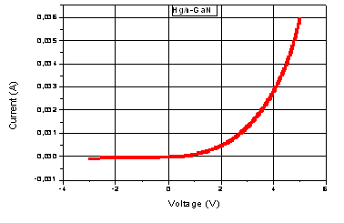
Figure 2. Characteristic I = f (V) of Hg / n-GaN structure.
For the determination of the electrical parameters, we exploit the general formula of the current which is of the following form [8]:
|
|
(1) |
where n is the ideality factor which is used to assess the quality of the metal semiconductor interface. The closer it is to 1 the characteristic of the current live will be close to the theoretical model, q is the electron charge (C), V is the applied voltage (V), k is the Boltzmann constant (1.3806·10-23 Jk-1), Ti s the temperature (in k) and IS is the saturation current given by (2).
|
IS = SA*T2exp(-qΦb/kT) |
(2) |
where S is the area of contact, q the electron charge, T is the temperature, k is Boltzmann's constant, A* is the Richardson's constant, Φb the barrier height and n is the ideality factor the diode.
From (1), we can draw the sin curve ln [I] as a function of bias voltage (V) (Figure 3).
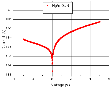
Figure 3. Changes of ln[I] according to the bias voltage.
The intersection of the interpolation line of the first linear region of the curve ln [I] = f (V) with the axis common to determine the saturation current Is and the ideality factor n of the structure.
The interpolation line has the equation Y = A + BX, and that in the first region, with [9]:
|
B = q/nkT |
(3) |
|
A = ln[IS] |
(4) |
The value of the saturation current Is obtained is 2.45×10⁻⁷ A, there is greater value to current saturation thermionic, this indicates the presence of another current level of our structure.
For the ideality factor n which reflects the difference between the behavior of a perfect structure and a real structure, the value obtained is 1.13.
We can express the barrier height Φb (originally zero polarization) by [9]:
|
|
(5) |
where A* is the Richardson's constant which is effectively equal to 26,438 A.cm-2.k-2[5], S is the surface of the pin of mercury which is equal to 7.85x10⁻³ cm2 end T is the temperature taken is equal to 300 k.
Replacing the value of the saturation current in the above equation, the value of ΦB obtained is 0.65 eV.
According to the characteristics ln [I] = f (V) we remark that the effect of the series resistance Rs cannot be neglected.
To calculate this parameter, we use the following equation [10]:
|
RS = ΔV/T |
(6) |
The estimated series resistance is 670 Ω.
The intersection of the interpolation line of the first linear region of the curve ln [I] = f (V) with the axis common to determine the saturation current Is and the ideality factor n of the structure.
Capacitance-voltage characterization
The following figure shows the characteristic (C-V) derived from measurements of the capacitance taken at 1 MHz. using a tester capacitance-voltage model "Keithley test system. 590 HP Scan".
The bench work automatically, it is constituted by an oscillator, phase detector, and a ramp generator, the whole is controlled by a computer connected via an interface card to the tester. The software adapted with the tester we facilitates handling, and the results are directly displayed on the monitor [7].
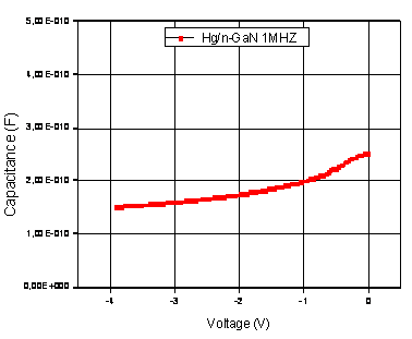
Figure 4. Characteristic capacitance-voltage of the Hg /n-GaN structure in high frequency (1MHz)
To calculate the diffusion voltage and doping we must trace the characteristic 1/C2 = f (V, Figure 5).
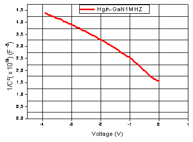
Figure 5. Characteristics of Hg / n-GaN structure 1/C2 = f (V) in high frequency
The curve is obtained with the appearance of a straight line. Knowing the equation of the line obtained by linear filtering performed using the software "Origin", we obtained a diffusion voltage Vd of the order of 1.11 V and a substrate doping Nd 1.68´1016 cm-3.
For the potential barrier, the value of Vd is introduced in (7) [11]:
|
|
(7) |

The value found of ΦB is 1.24 V.
Determining the density of interface states Nss
To evaluate the distribution of interface states Nss in the bandgap of the semiconductor (GaN) we calculated Nss (V) using the following expression [12]:
|
|
(8) |
with εi = 3.5ε0 the permittivity of the oxide layer (Ga2O3) and εs = 9.5ε0 the permittivity of the semiconductor.
The thickness δ of the oxide is about 23 Å and W is the depletion region which is of the order of 2630 Å. and the variation of the ideality factor (n) based on the bias voltage (V) is derived from the following equation:
|
|
(9) |
In an n-type semiconductor, the energy of the interface states Ess with respect to bottom of the conduction band at the surface of the semiconductor is given by:
|
EC-ESS = qΦe-qV |
(10) |
This relationship expresses the variation of the energy density of interface states ESS (referenced to the conduction band energy Ec) as a function of the bias voltage (V), resulting a variation of NSS according to (Ec-ESS):
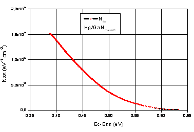
Figure 6. Representation of the variation of the density of interface states as a function of (Ec-Ess) diode Hg / n-GaN
The determined value of Nss(E) near the mid-gap is minimal was in the range of 1.85x1012cm-2 eV-1 , it has increased exponentially from 1.85x1012cm-2 eV-1 in (Ec-0,60) to 1.46x1014 cm-2 eV-1 in (Ec-0.39). The low surface state density on the studied sample shows the electronic quality of interface.
Conclusions
In this study, a of bulk gallium nitride Schottky diode has been fabricated and the I–V and C–V characteristics of this structure have been investigated. The values of the ideality factor, series resistance and barrier height have been calculated.
The electrical characterization (I-V) showed that our diode arranged a low saturation current but higher than the theoretical one due to the presence of other currents at our diode (tunneling current, leakage current), an ideality factor (n) is slightly greater than 1 because inhomogeneity of the surface of our diode.
The Characterization (C-V) shows the feasibility of electronic components with the bulk GaN. The barrier height determined by (I-V) is lower than that determined by (C-V) showing the thermionic effect plus other events (such as the tunneling leakage current).
Otherwise we observed the presence of a native oxide layer and an interface state density (Nss) slightly higher when approaching the conduction band.
Acknowledgements
This work was supported by the Laboratory of Applied Microelectronics, University Djillali Liabès of Sidi Bel Abbes, Algeria.
References
1. Johnson J. W., Zhang A. P., Luo W. B., Ren F., Pearton S. J., Park S. S., Park Y. J., Chyi J., Breakdown voltage and reverse recovery characteristics of free-standing GaN Schottky rectifiers, IEEE Trans. Electron Devices, 2002, 49(1), p. 32-36.
2. Wu Y.-F., Saxler A., Moore M., Smith R. P., Sheppard S., Chavarkar P. M., Wisleder T., Mishra U. K., Parikh P., 30-W/mm GaN HEMTs by field plate optimization, IEEE Electron Devices Lett., 2004, 25(3), 117-119.
3. Hacke P., Detchprohm T., Hiramatsu K., Sawaki N., Schottky barrier on n-type GaN grown by hydride vapor phase epitaxy, Appl. Phys. Lett., 1993, 63(19), p. 2676-2678.
4. Rhoderick E. H., Metal-Semiconductor Contacts, University Press, Oxford, 1988.
5. Sze S. M., Physics of semiconductor devices, John Wiley & Sons, New York, 1981.
6. Hongping Z., Ronald A. A., Yik-Khoon E., Nelson T., Optical gain analysis of strain-compensated InGaN-AlGaN quantum well active regions for lasers emitting at 420–500 nm, Opt Quant Electron, 2008, 40, p. 301-306.
7. Hudait M. K., Krupanidhi S. B., Interface statea density distribution in Au/n-GaAs Schottky diodes on n-Ge and n-GaAs substrates, Materials Science and Engineering, 2001, B87, p. 141-147.
8. Singh A., Time degradation of metal/CdF2 schottky diodes, Solid-State Electronics, 1983, 26(8), p. 815-817.
9. Wang Y. H., Houng M. P., Chen F. H., Sze P. W., Study of AuAgFe/AlGaAs Schottky diodes fabricated byin situ molecular beam epitaxy, Journal of Materials Science: Materials in Electronics, 1992, 3(4), p. 206-210.
10. Siva Pratap Reddy M., Rajagopal Reddy V., Choi C.-J., Electrical properties and interfacial reactions of rapidly annealed Ni/Ru Schottky rectifiers on n-type GaN, Journal of Alloys and Compounds, 2010, 503, p. 186-191.
11. Mathieu H., Physique des semiconducteurs et composants électroniques, 2009.
12. Card H. C., Rhoderic E. H., Studies of tunnel MOS diodes I. Interface effects in silicon Schottky diodes, J. Appl. Phyus., 1971, 4(10), p. 1589- 1602.